A 5V JTAG/SWD Level Shifter
Using some LSF0204D bidirectional level translators, I built some full JTAG level shifters for targets using 5 volts. I use a Bus Blaster which already has a flexible buffer capable of working anywhere from 1.5 to 3.3 volts, but I needed to debug a 5 volt target.
The design I settled on uses minimal, cheap support components. In fact the hardest component to source was the 20-pin right-angle female connector to connect it to the host.
Surprisingly rare connector
I made things harder on myself, refusing to use an unkeyed connector which could be inserted in reverse. But 20-pin JTAG headers are keyed for a reason. Reversed insertion would bridge most of the target's signal lines together with its VDD along with bridging all the host side signals to its VTG. Icky and potentially damaging, hence the requirement for a key.
After several days of searching, only one product fit the bill: Sullins SFH11-PBPC-D10-RA-BK. This is further perplexing since these connectors can be found on cheaply available JTAG breakouts/multi-adapter boards from China:
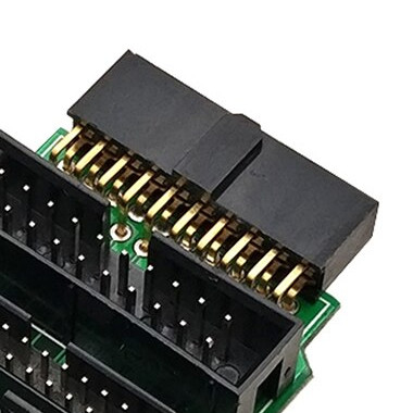
Perhaps I am missing some keyword, but all I could find from the regular China markets available to western hobbyists were unkeyed. I even asked on IRC and didn't get any further than I already had by myself - let me know if there's a better source for these, but I'm OK with the Sullins part from DigiKey for hobbyist work.
Board design
Shifters
In theory, 20-pin JTAG can be level shifted without the use of bidirectional level shifters since all signals have known directions. This would allow for the use of shifters with Schmitt-triggering inputs and strong drive strength, increasing the bus speeds at which the board could be used. However, some JTAG adapters support SWD, a protocol reducing the signal count, in part by making the data line bidirectional.
Instead of hoping to grasp some extra bandwidth at the cost of dealing with multiple shifter families, I settled on using the LSF family of shifters from Texas Instruments for all signals. Not only does it mean the layout is simpler with less chance of me locking myself out of some esoteric protocol that uses signal directions I didn't consider, but it can also make power supply simpler.
Power
I originally considered feeding the lower supply from a 3.3 volt LDO regulator fed from the target VDD in order to guarantee rail sequencing, which would allow me to use an advanced bidirectional level shifter (TXB0104), but decided against it for flexibility. The Bus Blaster JTAG adapter I use has an optional header to send 3.3 volts out its VTG, so I rely on this functionality. Simpler level shifters including the LSF have no rail sequence requirements, making it a perfect fit.
Misc layout
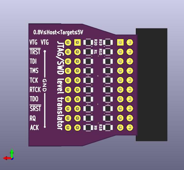
20-pin JTAG has all the interesting signals on one side of the connector, and puts 9 grounds and 1 VTG on the second row. By placing the through-hole headers both on the top side of the board, we keep the signal pins on the same side of their respective footprints as the LSFs. This makes routing simpler since the grounds get relegated to ground fill while the signals are a fairly simple fanout wasting only a single channel per chip.
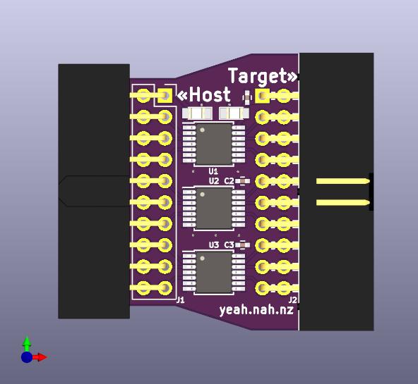
One indicator LED per rail is laid down, as well as a small 100 nF capacitor per LSF. On the rear of the board is room enough for our large, hand-soldering-friendly resistors:
- R1-R9 are identical pullups for the target side, and R10-R18 are a further set for the host side. I'm running with 1k for all 18 for now, requiring a not-too-unreasonable drive strength of about 8 mA for a 3.3 to 5V situation.
- R19 and R20 are current limiting resistors for the LEDs on the top side, 1.5k and 3.3k for approximately 1 mA of current (modern LEDs are crazy efficient).
These are all 2012 metric resistors, intentionally large (at least for surface mount) to encourage end-user experimentation with pullup values to best suit their own application.
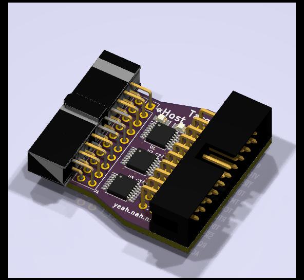
The obligatory raytrace shows the Kicad dev team's dedication to other, more important features, and/or the full evil of the colour-hacking I did on the STEP model in vim ☺
The whole board is designed to plug directly into a JTAG adapter such as the DP Bus Blaster which has a 20-pin boxed male header onboard. This level shifter then effectively extends the header just shy of 30 mm, intentionally introducing no right angles or other twists.
Finished assembly photos
To come!
Performance
Upshifting
This brings out the worst of the passive type of level shifter I am using here. However, the performance is still pretty good, thanks to the specially-designed FETs used in the LSF family. They appear to present a very low capacitance to the bus so that once the FET is turned off and we rely on the pullup to pull the high voltage bus the rest of the way up, it can do so relatively quickly.
It also looks like the VGSth of the FETs is exceedingly low, though I haven't yet measured this specifically at DC.
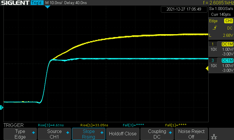
The falling edges are, as always, fairly sharp. Note that the bottom of the waveform is a little high, but still within 5 volt CMOS spec, and walking the line of TTL spec. This would be less of a problem with a lower impedance transmitter than the 50 ohm source seen here.
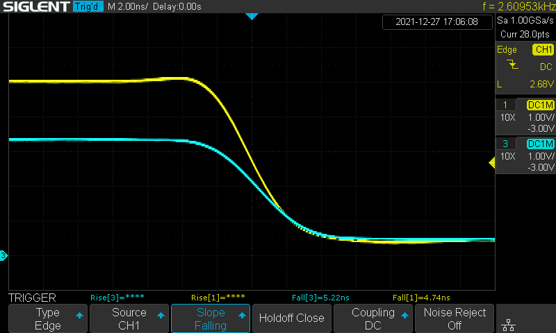
The propagation delay is minimal, approximately 1 ns.
Downshifting
Downshifting is a mostly breeze for this type of FET level shifter, since the FET can remain switched on throughout most of the duration of each type of edge. The only real concern is the VGSth of the FET, since a non-zero VGSth will cause the FET to turn off part-way through the rising edge, resulting in the slower pullup to raise the bus voltage the rest of the way. However, as noted above, it looks like the VGSth on the FETs in the LSF family is exceedingly low. This results in excellent edges almost undistorted by the level shifter.
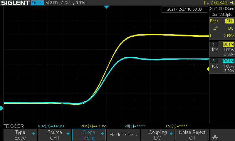
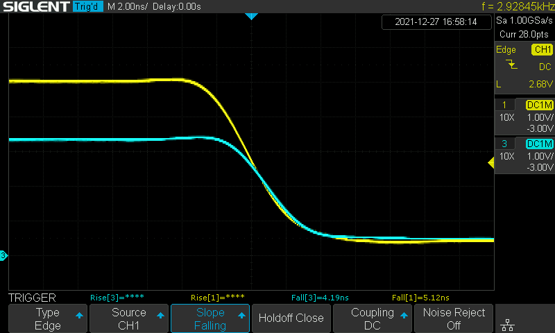
The propagation delay is marginally longer here, approximately 1.5 to 2 ns.
Testing and experience
One of the first things I did was to try and run the low side of this adapter down to 800 mV. This is technically undervolting the IO bank of the Xilinx XC2C32A on the Bus Blaster I was using, but it worked flawlessly like a champ. As the voltage difference between the two sides increases, upshifting slows down of course, but this is fully predictable.
I've used this level shifter for JTAGging various targets, including some iffy cases where host and target voltages are both 3.3 volts. This has helped in some cases where a target otherwise upsets the JTAG adapter. The LSF datasheet recommends keeping the B side (target) 0.8 to 1 volts higher than the A side (host), presumably to avoid false reverse direction triggers/clipping, but it appears to work well enough for medium speed JTAG 1–5 MHz with no issues. YMMV.
Things I still want to measure for fun:
- crosstalk between channels
- VGSth of FETs
Overall it's a nifty wee tool I like to keep in the JTAG box. Hopefully I find time to upload the design files, but I think it should be easy to reproduce from scratch for anyone, and could be a good starter project mixing simple SMT with through-hole.